- 您现在的位置:买卖IC网 > Sheet目录478 > MMA6331LT (Freescale Semiconductor)SENSORS ACCELEROMETER 14LGA
�� �
�
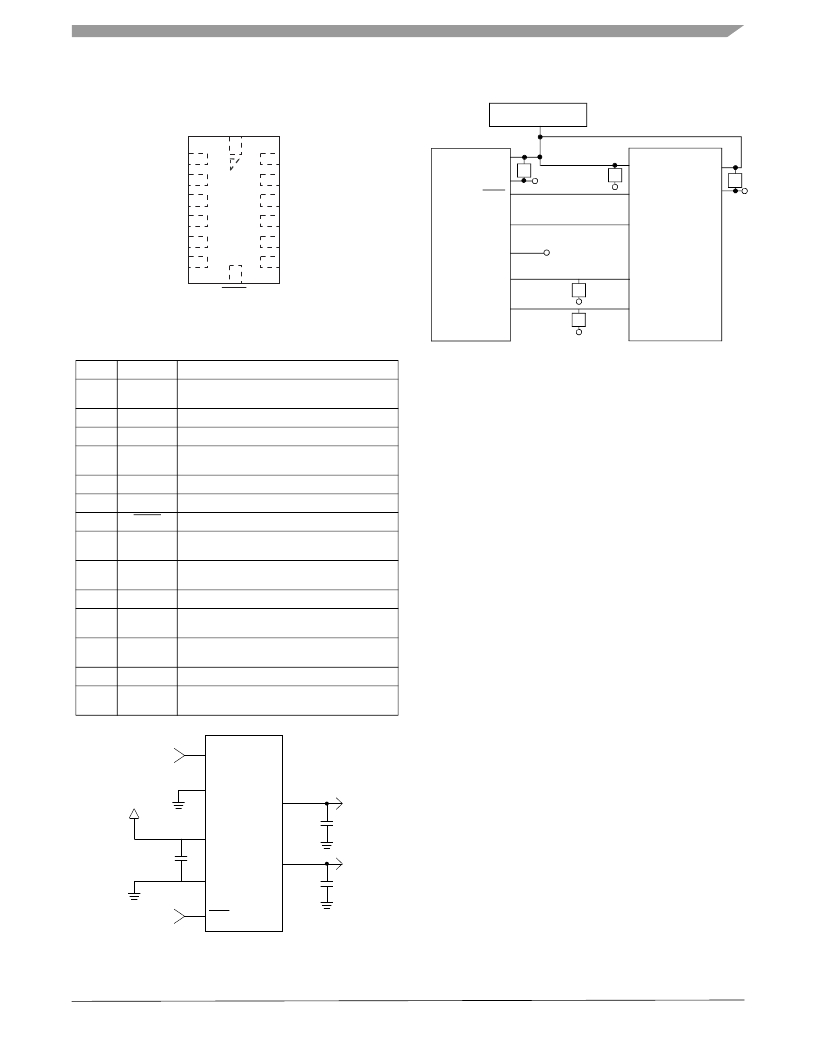
�BASIC� CONNECTIONS�
�Pin� Descriptions�
�Top� View�
�PCB� Layout�
�N/C�
�POWER� SUPPLY�
�N/C�
�X� OUT�
�Y� OUT�
�GND�
�N/C�
�N/C�
�V� DD�
�V� SS�
�Sleep�
�C�
�C�
�V� RH�
�P0�
�V� DD�
�V� SS�
�C�
�N/C�
�V� SS�
�V� DD�
�g-Select�
�N/C�
�N/C�
�g-Select�
�GND�
�P1�
�Sleep�
�Figure� 4.� Pinout� Description�
�X� OUT�
�Y� OUT�
�C�
�C�
�A/D� IN�
�A/D� IN�
�Table� 4.� Pin� Descriptions�
�Pin� No.� Pin� Name�
�Description�
�Figure� 6.� Recommended� PCB� Layout� for� Interfacing�
�1�
�2�
�3�
�4�
�5�
�6�
�7�
�8�
�9�
�10�
�11�
�12�
�13�
�14�
�N/C�
�X� OUT�
�Y� OUT�
�N/C�
�V� SS�
�V� DD�
�Sleep�
�N/C�
�N/C�
�g-Select�
�N/C�
�N/C�
�GND�
�N/C�
�No� internal� connection�
�Leave� unconnected�
�X� direction� output� voltage�
�Y� direction� output� voltage�
�No� internal� connection�
�Leave� unconnected�
�Power� Supply� Ground�
�Power� Supply� Input�
�Logic� input� pin� to� enable� product� or� Sleep� Mode�
�No� internal� connection�
�Leave� unconnected�
�No� internal� connection�
�Leave� unconnected�
�Logic� input� pin� to� select� g� level�
�Unused� for� factory� trim�
�Leave� unconnected�
�Unused� for� factory� trim�
�Leave� unconnected�
�Connect� to� Ground�
�Unused� for� factory� trim�
�Leave� unconnected�
�Accelerometer� to� Microcontroller�
�NOTES:�
�1.� Use� 0.1� μF� capacitor� on� V� DD� to� decouple� the� power�
�source.�
�2.� Physical� coupling� distance� of� the� accelerometer� to�
�the� microcontroller� should� be� minimal.�
�3.� Place� a� ground� plane� beneath� the� accelerometer� to�
�reduce� noise,� the� ground� plane� should� be� attached� to�
�all� of� the� open� ended� terminals� shown� in� Figure� 6� .�
�4.� Use� a� 3.3� nF� capacitor� on� the� outputs� of� the�
�accelerometer� to� minimize� clock� noise� (from� the�
�switched� capacitor� filter� circuit).�
�5.� PCB� layout� of� power� and� ground� should� not� couple�
�power� supply� noise.�
�6.� Accelerometer� and� microcontroller� should� not� be� a�
�high� current� path.�
�7.� A/D� sampling� rate� and� any� external� power� supply�
�switching� frequency� should� be� selected� such� that�
�they� do� not� interfere� with� the� internal� accelerometer�
�sampling� frequency� (11� kHz� for� the� sampling�
�frequency).� This� will� prevent� aliasing� errors.�
�Logic�
�Input�
�10�
�g-Select�
�8.� 10� M� Ω� or� higher� is� recommended� on� X� OUT� and� Y� OUT�
�VDD�
�13�
�6�
�MMA6331L�
�GND�
�XOUT�
�VDD�
�2�
�3.3� nF�
�to� prevent� loss� due� to� the� voltage� divider� relationship�
�between� the� internal� 32� k� Ω� resistor� and� the�
�measurement� input� impedance.�
�0.1� μF�
�5�
�VSS�
�YOUT�
�3�
�3.3� nF�
�Logic�
�Input�
�7�
�Sleep�
�Figure� 5.� Accelerometer� with� Recommended�
�Connection� Diagram�
�MMA6331L�
�Sensors�
�Freescale� Semiconductor�
�5�
�发布紧急采购,3分钟左右您将得到回复。
相关PDF资料
MMA6341LT
IC ACCELER 3G/8G XY-AXIS 14LGA
MMA6361LT
IC ACCELER 1.5G XY-AXIS 14LGA
MMA6527KW
IC ACCELEROMETER XY AXIS 16QFN
MMA6556KW
IC ACCELEROMETER X AXIS 16QFN
MMA6826AKW
IC ACCELEROMETER XY AXIS 16QFN
MMA6854KW
IC ACCELEROMETER X AXIS 16QFN
MMA7331LR2
ACCELEROMETER 4G XYZ ENH 14-LGA
MMA8451QT
IC ACCELEROMETER 3AXIS 16QFN
相关代理商/技术参数
MMA6341LR1
功能描述:加速计 - 板上安装 3g-8g XY-Axis Low g RoHS:否 制造商:Murata 传感轴:Double 加速:12 g 灵敏度: 封装 / 箱体: 输出类型:Analog 数字输出 - 位数:11 bit 电源电压-最大:5.25 V 电源电压-最小:4.75 V 电源电流:4 mA 最大工作温度:+ 125 C 最小工作温度:- 40 C
MMA6341LR2
功能描述:加速计 - 板上安装 3G-9G XY-AXIS LOW G RoHS:否 制造商:Murata 传感轴:Double 加速:12 g 灵敏度: 封装 / 箱体: 输出类型:Analog 数字输出 - 位数:11 bit 电源电压-最大:5.25 V 电源电压-最小:4.75 V 电源电流:4 mA 最大工作温度:+ 125 C 最小工作温度:- 40 C
MMA6341LT
功能描述:加速计 - 板上安装 3G-9G XY-AXIS LOW G RoHS:否 制造商:Murata 传感轴:Double 加速:12 g 灵敏度: 封装 / 箱体: 输出类型:Analog 数字输出 - 位数:11 bit 电源电压-最大:5.25 V 电源电压-最小:4.75 V 电源电流:4 mA 最大工作温度:+ 125 C 最小工作温度:- 40 C
MMA6361L
制造商:FREESCALE 制造商全称:Freescale Semiconductor, Inc 功能描述:?±1.5g, ?±6g Two Axis Low-g Micromachined Accelerometer
MMA6361LR1
功能描述:加速计 - 板上安装 1.5 XY LGA 14 LD ENH RoHS:否 制造商:Murata 传感轴:Double 加速:12 g 灵敏度: 封装 / 箱体: 输出类型:Analog 数字输出 - 位数:11 bit 电源电压-最大:5.25 V 电源电压-最小:4.75 V 电源电流:4 mA 最大工作温度:+ 125 C 最小工作温度:- 40 C
MMA6361LR2
功能描述:加速计 - 板上安装 1.5 XY LGA 14 LD ENH RoHS:否 制造商:Murata 传感轴:Double 加速:12 g 灵敏度: 封装 / 箱体: 输出类型:Analog 数字输出 - 位数:11 bit 电源电压-最大:5.25 V 电源电压-最小:4.75 V 电源电流:4 mA 最大工作温度:+ 125 C 最小工作温度:- 40 C
MMA6361LT
功能描述:加速计 - 板上安装 1.5G XY LGA 14 LDS ENH RoHS:否 制造商:Murata 传感轴:Double 加速:12 g 灵敏度: 封装 / 箱体: 输出类型:Analog 数字输出 - 位数:11 bit 电源电压-最大:5.25 V 电源电压-最小:4.75 V 电源电流:4 mA 最大工作温度:+ 125 C 最小工作温度:- 40 C
MMA6519KW
功能描述:加速计 - 板上安装 XY-AXIS 80/ 80G RoHS:否 制造商:Murata 传感轴:Double 加速:12 g 灵敏度: 封装 / 箱体: 输出类型:Analog 数字输出 - 位数:11 bit 电源电压-最大:5.25 V 电源电压-最小:4.75 V 电源电流:4 mA 最大工作温度:+ 125 C 最小工作温度:- 40 C